Creating a Silicon Solar Cell in Open Research Laboratory
This documentation provides a detailed overview of a silicon solar cell desinged and tested in the Open Research Laboratory.
It includes the objectives of the study, the solar cell stack, testing results, and interactive tabs for experimental curves.
About the Solar Cell
The cell is a monocrystalline silicon solar cell, optimized for high efficiency using standard layers including anti-reflective coating, passivation layers, and front/rear contacts. This solar cell is designed and tested in the Open Research Laboratory.
Objectives of this Research
The main objectives of this experiment are:
- To simulate and measure the IV curve of the silicon solar cell under controlled laboratory conditions.
- To calculate the efficiency of the solar cell in different environmental factors such as humidity, temperature, and light intensity.
- To evaluate the influence of layer thickness and material properties on the performance of the solar cell.
Solar Cell Stack Configuration
| Layer Name | Material | Thickness | Structure | Bandgap | Purpose |
|---|---|---|---|---|---|
| Anti-Reflective Coating (ARC) | Si₃N₄ | 70 nm | PECVD thin film | 5.3 eV | Maximize light absorption |
| Front Contact (Metal Grid + TCO) | ITO (100 nm) + Silver grid (3 µm) | 100 nm / 3 µm | Transparent conductive oxide + metal fingers | 3.5 eV | Conduct electricity with minimal shading |
| Passivation Layer | Al₂O₃ | 30 nm | Covers emitter layer | 6.5 eV | Reduce surface recombination |
| n-type Emitter Layer | Phosphorus-doped silicon | 1 µm | Heavily doped top layer | 1.12 eV | Generate electrons and form p-n junction |
| p-type Base Layer | Boron-doped silicon | 180 µm | Bulk wafer | 1.12 eV | Collect holes and provide mechanical support |
| Rear Passivation Layer | SiO₂ | 70 nm | Full back coverage | 9 eV | Minimize back surface recombination |
| Back Contact | Aluminum | 150 nm | Full-area metallization | 0 eV | Complete circuit and reflect unabsorbed light |
Creating in ORL
To create this experiment in open research laboratory, we have used the following:
- Components
- Research Details
Components we have used
{
  "Anti-Reflective Coating (ARC)": {
    "Material": "Si₃N₄",
    "Thickness": "70 nm",
    "Structure": "PECVD thin film",
    "Bandgap": "5.3 eV",
    "Purpose": "Reduce reflection, maximize light absorption"
  },
  "Front Contact (Metal Grid + TCO)": {
    "Material": "ITO (100 nm) + Silver grid (3 µm)",
    "Structure": "Transparent conductive oxide with metal fingers",
    "Bandgap": "3.5 eV",
    "Purpose": "Conduct electricity while allowing light to pass"
  },
  "Passivation Layer": {
    "Material": "Al₂O₃",
    "Thickness": "30 nm",
    "Structure": "Covers emitter layer except contacts",
    "Bandgap": "6.5 eV",
    "Purpose": "Reduce surface recombination"
  },
  "n-type Emitter Layer": {
    "Material": "Phosphorus-doped silicon",
    "Thickness": "1 µm",
    "Structure": "Heavily doped top surface",
    "Bandgap": "1.12 eV",
    "Purpose": "Generate electrons, form p-n junction"
  },
  "p-type Base Layer": {
    "Material": "Boron-doped silicon",
    "Thickness": "180 µm",
    "Structure": "Bulk lightly doped wafer",
    "Bandgap": "1.12 eV",
    "Purpose": "Collect holes, provide mechanical support"
  },
  "Rear Passivation Layer": {
    "Material": "SiO₂",
    "Thickness": "70 nm",
    "Structure": "Full coverage at wafer back",
    "Bandgap": "9 eV",
    "Purpose": "Reduce back-surface recombination"
  },
  "Back Contact": {
    "Material": "Aluminum",
    "Thickness": "150 nm",
    "Structure": "Full-area metal contact",
    "Bandgap": "0 eV",
    "Purpose": "Complete circuit, reflect unabsorbed light"
  }
}
Research Description
this is a basic silicon solar cell, find out the efficiency of conversion rate and other things. this cell is 2*2 cm. find the stability of the layers due to humidity and other factors. Make IV graph and conversion rate graph + efficiency graph too.
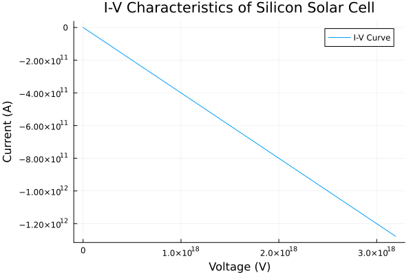
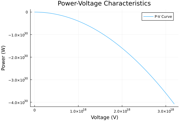
Results we got
- I-V Curve
- Power Curve
Run Workflow
If you want to replicate this experiment or customize it, we have made the workflow publicly available in our Open Research Laboratory. You can:
- Run a Copy: Simply click on Run a Copy of our QKD workflow.
- Modify & Execute: Make any desired modifications and execute the experiment on your own.
This allows you to leverage our pre-configured setup without starting from scratch.
- Visit Open Research Laboratory.
- Navigate to the Workflows page.
- Select the Silicon Solar Cell Workflow.
- Click on Run – this will create a duplicate of the workflow for your use.
- Run the experiment directly on your virtual lab environment.